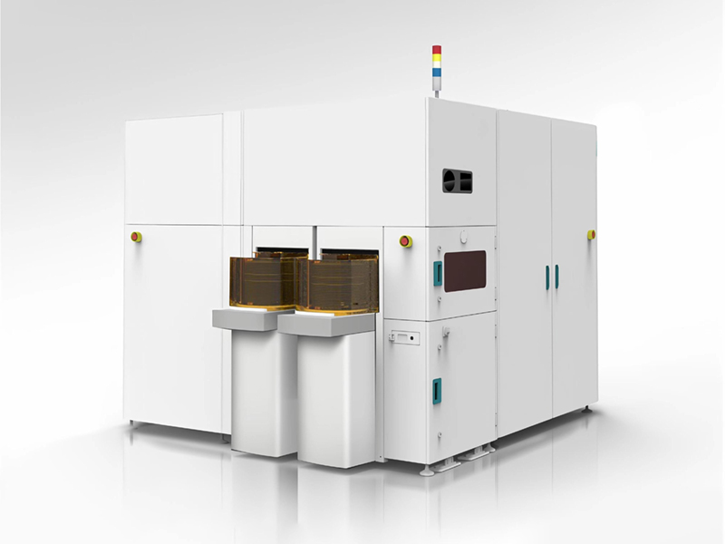
Our Critical Dimension Scanning Electron Microscope (CD-SEM) product achieves the measurement of the critical dimensions (CD) at lithography and etching process steps within an IC manufacturing process, thereby ensuring healthy process monitoring, as well as yield enhancement. It does this via the high throughput nano-scale imaging of patterned wafers using high-resolution-low-voltage scanning electron microscope technology. Our CD-SEMs are comparable with mainstream offerings which are already widely used in the semiconductor industry, and furthermore, they are integrated with unique innovative techniques, making breakthroughs in charge control, positioning accuracy, sampling speed, etc, and can cover the matured processes above 28 nanometers for 6/8/12-inch silicon, silicon carbide, gallium nitride, sapphire and other substrates.
Highlights:EOS column is designed with independent intellectual property for meeting the specialized needs of CD measurement; Up-to-date electrical deflection system and matching high-speed image channel facilitate high throughput (WPH); High accuracy position tracking system makes pattern matching easy or even unnecessary; Patented modulation scanning technique enables higher accuracy measurement to cover more difficult scenarios.


